Technology
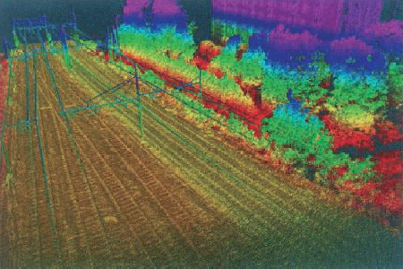
LiDAR stands for Light Detection And Ranging or Light imaging, Detection And Ranging. It emits laser pulse and detects the bounced back signal from objects. By extracting the distance and relative velocity to objects from the signal, and steering the beam to different directions, the 3D model of the environments is constructed, and represented by the data called "point cloud". LiDAR is divided into three types and they are listed below
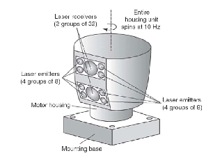
Conventionally scanning LiDAR uses mechanical rotation to spin the sensor for 360 degree detection. LiDAR with mechanical rotation enables high speed scanning and is safer for eyes even with higher power laser as the light does not goes to only one direction.
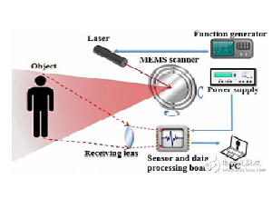
Hybrid solid state LiDAR uses micro-electromechanical system (MEMS) technology in which a MEMS based mirror moves to “scan” the environment. The technology outpaces mechanical rotation in price and size but is short in long distance detection.
Solid state means the LiDAR doesn't contain any moving part. Correspondingly, soild state beam steering means the beam propagation direction is controlled without any moving parts,which include wavelength-tuning dispersion, optical-lens switch and optical phased array (OPA).
Three mechanisms for solid state beam steering are wavelength-tuning dispersion, optical-lens switch and optical phased array (OPA).
Dispersion
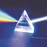
Wavelength-tuning dispersion is a true solid-state approach. However, due to the limitation of wavelength tuning range, this procedure is practically one-dimensional.
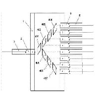
Opical-lens switch steers the beam by switching the emitting position of light on the focal plane of a lens. Similar to OPA, integration scale and optical loss matters in this technology.
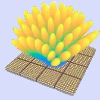
Optical Phased Arrays (OPA) describes a control of the phase and amplitude of light propagating through. This shape is also a solid-state concept. Sidelobes, integration scale and optical power loss are the challenges in OPA technology.
FMCW stands for Frequency Modulated Continuous Wave. FMCW lidar sends out a constant stream of light (“continuous-wave”) and changes the frequency of that light at regular intervals (“frequency-modulated”). This allows us to both determine the location of objects and precisely measure their velocity using the Doppler effect.
DSP stands for Digital Signal Processing. With Digital Signal Processing, you can manipulate signals after they have been converted from analog voltages and currents into digital form -- i.e., as numbers. Normal analog operations of filtering, mixing, and signal detection all have their parallels in the DSP world. Because the cost of complex digital processing is very low, DSP is often the preferred way to build high-performance communications and sensing systems.
Silicon Photonics is a combination of two of the most important inventions in the 20th century—the silicon integrated circuit and the semiconductor laser and optical devices. It enables faster data transfer over longer distances compared to traditional electronics, while utilizing the efficiencies of high-volume silicon manufacturing. Thousands or even more optical devices are integrated compactly on a single chip.
- Solid state Lidar can provide increased range and resolution required for high-speed driving.
- Increased precision through long-range detection can help better classify objects (such as pedestrians and vehicles) and improve tracking of movement (for instance, how fast a pedestrian is moving and in which direction).
- Because it has no moving parts, a solid-state device is immune to shock and vibration and thus less prone to motion blur. It also helps to save construction space within the scanners, allowing them to reach extremely small dimensions and to cut costs.
- Solid state device with low power consumption could run without failure up to 100x longer, as it has a lifespan of up to 100,000 hours. In other words, it's likely to outlive your car, making it more durable and more reliable.